
Semiconductor Industry
Precision support for fabs handling high-value and sensitive equipment.
Expertise for Semiconductor.
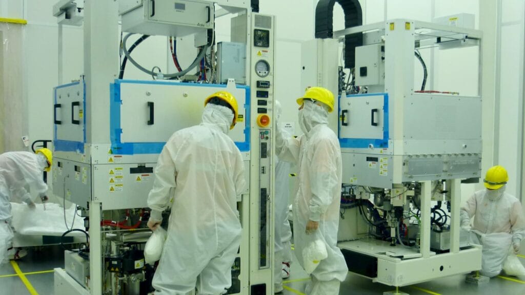
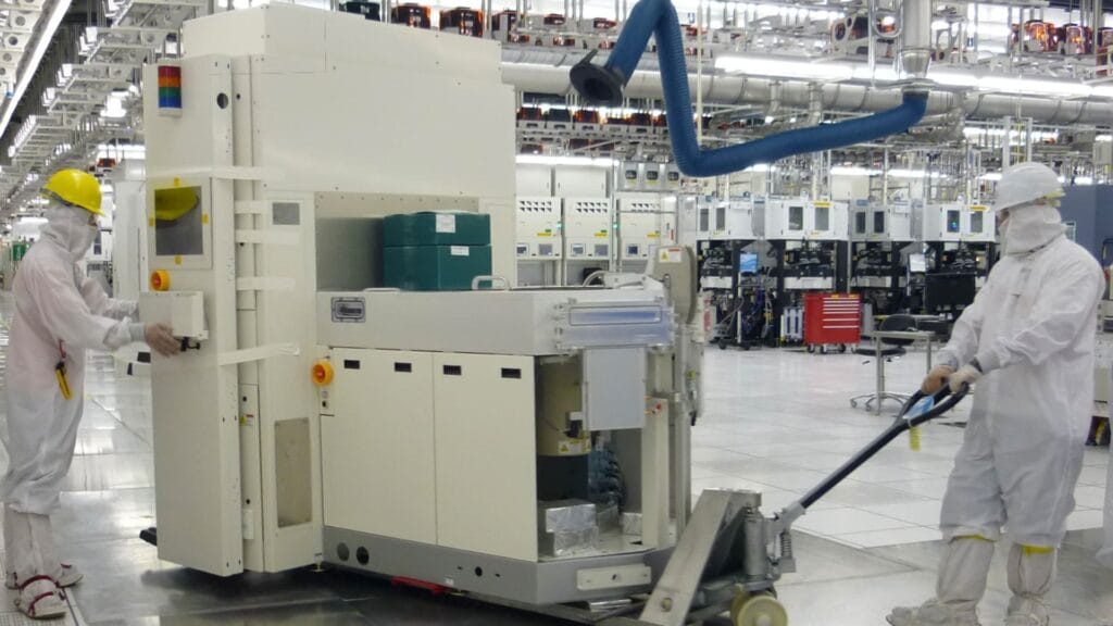
B H S works inside active semiconductor fabs where equipment is sensitive, high value, and handled under strict control. Our teams support tool moving, installation, de-installation, AMHS work, and cleanroom operations across markets such as Singapore, Taiwan, the United States, and the Netherlands.
What we support.
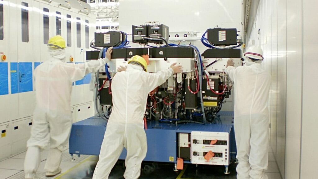
- Tool moving and placement
- Tool installation (non-commissioning)
- Tool de-installation and removal
- Photolithography tool moves and installs
- Metrology tool relocation
- AMHS installations and de-installations
- Cleanroom-compatible handling and rigging
- Crating and export packing for tools
- Vibration-controlled transport
- Controlled storage for fab equipment
- Datum marking and installation layout preparation
How we work in your environment.
- Gowning and cleanroom protocols for active fabs
- Controlled-environment workflows to reduce contamination risk
- Vibration, tilt, and movement control during handling
- Mechanical de-installation without chemical or process work
- Installation-ready placement aligned to fab layouts
- Coordination with fab engineering, facilities, and OEM teams
- Multi-market capability for cross-border fab support
Where we support your projects.
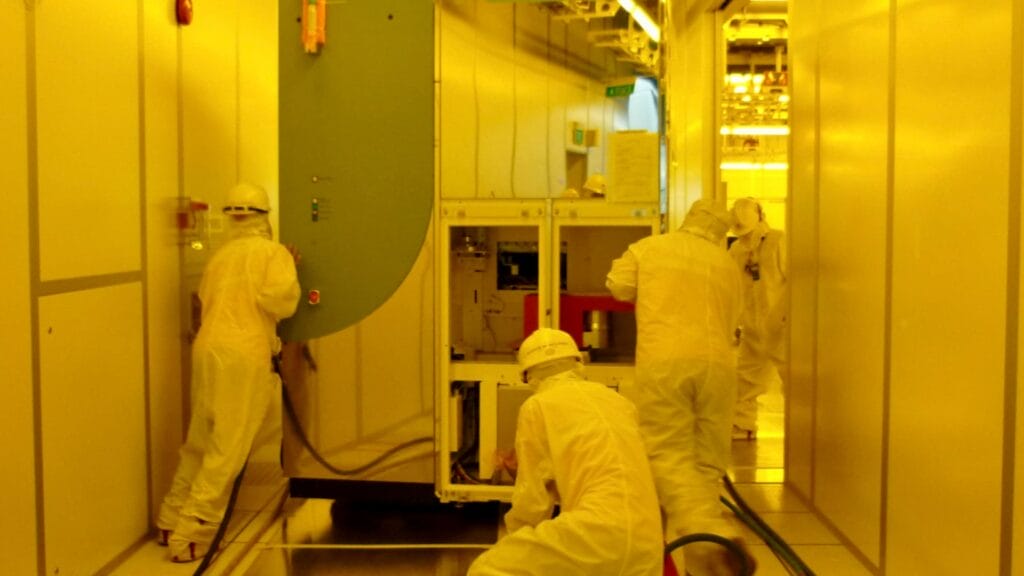
- Active tool bays
- Subfab access for mechanical disconnection
- Cleanroom-controlled zones
- Tool consolidation areas
- Packing and crating zones
- Cross-border deployments
Why customers choose B H S.
- Proven experience with sensitive semiconductor tools
- Disciplined teams trained for cleanroom environments
- Precision handling for photolithography and metrology equipment
- Consistency across markets with ISO-aligned methods
- Vibration-controlled transport for high-value tools
- Installation-ready positioning with datum marking
- Reliable planning and execution in active fab conditions
